Wafer Fabrication Equipment Guide: Explore Types, Processes, and Industry Applications
Wafer fabrication equipment plays an essential role in the semiconductor industry. It supports the production of integrated circuits, microprocessors, memory chips, sensors, and other electronic components used in modern technology. From smartphones and computers to automobiles, communication networks, medical devices, and industrial automation systems, semiconductor components are present in many aspects of everyday life.
A semiconductor wafer is a thin, circular slice of semiconductor material, usually silicon, on which electronic circuits are created. During manufacturing, the wafer passes through several highly controlled processes that form microscopic structures and electrical connections. These processes require specialised equipment capable of maintaining accuracy, cleanliness, temperature control, and consistent production conditions.
Wafer fabrication equipment includes machines used for cleaning, oxidation, deposition, photolithography, etching, ion implantation, polishing, inspection, and measurement. Each category performs a specific function in transforming a prepared wafer into a semiconductor device.
Understanding Semiconductor Manufacturing Equipment helps explain how electronic components are developed and why advanced wafer processing technology is important for the global electronics industry.
Importance of Wafer Fabrication Equipment in Semiconductor Manufacturing
Semiconductor manufacturing depends on precision, repeatability, and controlled processing conditions. Even small variations during fabrication can affect the electrical characteristics and reliability of a finished chip.
Wafer fabrication equipment supports the manufacturing process in several important ways.
Precision in circuit formation: Semiconductor devices contain extremely small structures. Advanced equipment helps create patterns and material layers with precise dimensions.
Consistent production quality: Automated systems maintain repeatable processing conditions across multiple wafers, helping manufacturers achieve consistent results.
Improved manufacturing efficiency: Modern semiconductor production equipment integrates automation, process monitoring, and material handling to support complex manufacturing operations.
Advanced chip development: New generations of processors, memory devices, and specialised integrated circuits require sophisticated fabrication technologies.
Contamination control: Semiconductor manufacturing takes place in highly controlled environments. Specialised cleaning systems, filtration equipment, and wafer-handling robots help reduce contamination risks.
Support for emerging technologies: Artificial intelligence, electric vehicles, cloud computing, telecommunications, and connected devices continue to increase demand for advanced semiconductor components.
Major Types of Wafer Fabrication Equipment
Wafer fabrication involves numerous specialised machines. Each machine performs a particular operation and contributes to the overall manufacturing sequence.
1. Photolithography Equipment
Photolithography equipment is used to transfer circuit patterns onto the surface of a semiconductor wafer. It is one of the most important technologies in semiconductor fabrication.
The process generally involves applying a light-sensitive material called photoresist to the wafer. A patterned mask or reticle is then used to expose selected areas to light. The exposed or unexposed portions are developed to create a pattern that guides subsequent manufacturing operations.
Important components include:
Wafer alignment systems.
Light sources and optical systems.
Photoresist coating equipment.
Exposure systems.
Development equipment.
Precision positioning stages.
Advanced photolithography systems use sophisticated optical technologies to create increasingly small circuit features. Extreme ultraviolet (EUV) lithography is used for certain advanced semiconductor manufacturing processes, while deep ultraviolet (DUV) systems remain widely used across different technology generations.
2. Etching Equipment
Etching equipment removes selected materials from the wafer surface to create patterns and structures.
The process is commonly divided into two main categories.
Wet etching: Uses chemical solutions to remove particular materials. It is often used when chemical selectivity and suitable material removal characteristics are required.
Dry etching: Uses gases, plasma, or reactive chemical species to remove material. Plasma-based techniques provide greater control over the shape and direction of material removal.
Common applications include:
Creating transistor structures.
Defining circuit patterns.
Forming contact openings.
Removing unwanted material layers.
Developing microscopic semiconductor features.
Etching accuracy is important because the final device structure depends on the dimensions and arrangement of the patterned materials.
3. Deposition Equipment
Deposition equipment creates thin films of materials on the wafer surface. These layers may provide electrical, insulating, protective, or structural functions.
Several deposition technologies are used in semiconductor manufacturing.
Chemical Vapour Deposition (CVD): Uses chemical reactions involving gases to form thin material layers on a wafer.
Physical Vapour Deposition (PVD): Uses physical processes to transfer material from a source onto the wafer surface.
Atomic Layer Deposition (ALD): Creates thin films through controlled, sequential surface reactions. It is particularly useful when highly controlled film thickness and coverage are required.
Deposition processes are used to create insulating layers, conductive films, barriers, and other structures required for integrated circuits.
4. Oxidation Equipment
Oxidation equipment forms oxide layers on semiconductor wafer surfaces. Silicon oxidation is an important process because silicon dioxide can function as an insulating or protective material.
The process generally involves exposing the wafer to oxygen or water vapour under controlled temperature conditions.
Important applications include:
Forming insulating layers.
Surface protection.
Electrical isolation.
Supporting specific device fabrication processes.
Creating oxide structures for semiconductor components.
Oxidation systems require accurate temperature management and controlled processing environments to achieve consistent material properties.
5. Ion Implantation Equipment
Ion implantation equipment introduces selected impurity atoms into semiconductor materials to modify their electrical characteristics.
This process is essential for controlling how semiconductor devices conduct electricity.
The equipment typically includes:
Ion sources.
Mass analysers.
Acceleration systems.
Beam scanning mechanisms.
Wafer handling systems.
Process monitoring equipment.
Ion implantation allows manufacturers to control the concentration and distribution of dopants within different wafer regions. These characteristics influence the performance of transistors, diodes, and other semiconductor structures.
6. Chemical Mechanical Planarization Equipment
Chemical Mechanical Planarization (CMP) equipment is used to create smooth and relatively flat wafer surfaces.
During semiconductor fabrication, multiple layers of materials are deposited and patterned. These operations can create uneven surface topography. CMP combines chemical reactions with mechanical polishing to remove selected material and improve surface uniformity.
Major components include:
Polishing pads.
Slurry delivery systems.
Wafer carriers.
Pressure control systems.
Cleaning units.
Process monitoring systems.
Planarization is important for subsequent lithography and deposition operations because surface irregularities can affect manufacturing accuracy.
7. Wafer Cleaning Equipment
Wafer cleaning equipment removes particles, chemical residues, organic contamination, and unwanted materials from wafer surfaces.
Contamination can interfere with circuit formation and negatively affect semiconductor device quality. For this reason, cleaning is performed at multiple stages throughout wafer manufacturing.
Common cleaning approaches include:
Wet chemical cleaning.
Deionised water rinsing.
Megasonic cleaning.
Solvent-based cleaning.
Dry cleaning techniques.
Modern cleaning systems are designed to handle wafers carefully while maintaining strict contamination-control conditions.
8. Inspection and Metrology Equipment
Inspection and metrology equipment evaluates wafer quality and measures important physical characteristics during production.
Inspection systems identify defects, particles, surface irregularities, and pattern problems. Metrology systems measure dimensions, film thickness, alignment, and other process characteristics.
Common equipment categories include:
Optical inspection systems.
Electron-beam inspection systems.
Film thickness measurement equipment.
Critical dimension measurement systems.
Surface analysis instruments.
Wafer defect detection systems.
These technologies help manufacturers monitor process performance and identify manufacturing problems before they affect a larger production batch.
Semiconductor Wafer Processing: Step-by-Step Manufacturing Process
Wafer fabrication is a multi-stage process in which different equipment categories work together. The exact manufacturing sequence depends on the semiconductor device, material system, and technology requirements.
The following stages provide a general overview.
1. Silicon Wafer Preparation
The process begins with a semiconductor substrate, commonly made from high-purity silicon.
Silicon is processed into an ingot, which is sliced into thin wafers. These wafers undergo grinding, polishing, cleaning, and inspection to achieve the required dimensions and surface quality.
Silicon Wafer Manufacturing Equipment supports these preparation operations.
2. Wafer Cleaning
Before additional processing, the wafer surface must be free from unwanted particles and contaminants.
Cleaning systems remove residues and prepare the surface for subsequent fabrication operations. Cleaning may be repeated throughout the manufacturing process.
3. Oxidation and Thin-Film Formation
Selected material layers are created through oxidation and deposition processes.
These layers may serve as insulators, conductors, barriers, or structural elements. The material composition and thickness depend on the device design.
4. Photolithography
Photolithography transfers the required circuit patterns onto the wafer.
Photoresist is applied, exposed through an optical system, and developed. The resulting pattern determines which regions will undergo subsequent material processing.
5. Etching
Etching removes selected portions of material according to the patterned layout.
This operation creates openings, trenches, and other structures needed for semiconductor devices.
6. Doping and Ion Implantation
Selected wafer regions receive controlled quantities of dopant atoms.
These impurities change the electrical properties of the semiconductor and help form the functional regions of electronic components.
7. Planarization
Chemical Mechanical Planarization improves surface flatness after selected deposition and patterning operations.
This helps prepare the wafer for additional layers and manufacturing stages.
8. Repeated Layer Formation
Modern integrated circuits contain numerous interconnected material layers and microscopic structures.
Deposition, lithography, etching, cleaning, and other processes may be repeated many times to create the complete device architecture.
9. Inspection and Quality Control
Inspection and metrology equipment evaluates wafer characteristics at different manufacturing stages.
Measurements and defect analysis help manufacturers monitor production quality and identify process variations.
10. Wafer Testing and Further Processing
After front-end fabrication, wafers undergo electrical testing to identify functional and defective semiconductor devices.
The wafers are subsequently transferred to packaging operations, where individual chips are separated, assembled, and prepared for use in electronic systems.
Major Applications of Wafer Fabrication Equipment
Wafer fabrication technology supports a wide range of industries. Semiconductor devices produced through these processes form the foundation of modern electronics.
1. Consumer Electronics
Smartphones, laptops, tablets, smart televisions, digital cameras, and wearable devices depend on semiconductor components.
Wafer fabrication equipment supports the development of processors, memory chips, display controllers, power management devices, and communication components.
2. Automotive Industry
Modern vehicles use semiconductor components in engine management, safety systems, infotainment, navigation, battery management, and driver-assistance technologies.
Electric vehicles and advanced automotive electronics require specialised power semiconductors, sensors, microcontrollers, and control processors.
3. Telecommunications
Telecommunication networks rely on semiconductor devices for signal processing, wireless communication, optical networking, and data transmission.
Wafer fabrication supports components used in mobile networks, base stations, routers, switches, and communication infrastructure.
4. Artificial Intelligence and Data Centres
Artificial intelligence applications require substantial computing capacity. GPUs, specialised AI accelerators, memory devices, and high-speed networking components are essential for modern data centres.
Advanced wafer fabrication technology enables the production of increasingly complex processors and semiconductor devices used in AI systems.
5. Healthcare and Medical Electronics
Medical electronics use semiconductor components in diagnostic equipment, patient monitoring systems, imaging devices, laboratory instruments, and wearable health technologies.
Specialised sensors and integrated circuits help electronic medical equipment process and transmit information.
6. Industrial Automation
Industrial systems use semiconductor devices in robotics, motor controllers, sensors, power electronics, and automated production equipment.
Wafer fabrication supports the development of electronic components used in manufacturing plants, energy systems, and industrial monitoring applications.
Semiconductor Manufacturing Technology: Important Developments
Semiconductor Manufacturing Technology continues to evolve as electronic devices become more complex and computing requirements increase.
Several developments are influencing modern wafer fabrication.
1. Extreme Ultraviolet Lithography
Extreme ultraviolet lithography uses very short-wavelength light to create extremely small circuit patterns. It is an important technology for certain advanced semiconductor manufacturing processes.
EUV systems involve sophisticated optics, specialised light sources, precision wafer stages, and tightly controlled operating environments.
2. Advanced Packaging Integration
Semiconductor development increasingly involves combining multiple chips or chiplets within a single package.
Technologies such as 2.5D and 3D integration support high-density connections between semiconductor components. These approaches can improve system integration and help address performance and power requirements.
3. Gate-All-Around Transistor Structures
Gate-All-Around (GAA) transistor architectures represent an important development in advanced transistor design.
Unlike traditional FinFET structures, GAA designs surround the transistor channel with gate material. This architecture provides improved electrostatic control and supports continued semiconductor scaling.
Manufacturing these structures requires advanced deposition, etching, lithography, and metrology equipment.
4. Silicon Carbide and Gallium Nitride Technologies
Silicon carbide (SiC) and gallium nitride (GaN) are wide-bandgap semiconductor materials used in specialised electronic applications.
They are particularly relevant to power conversion, electric vehicles, charging infrastructure, renewable energy systems, and high-frequency electronics.
Their manufacturing processes require specialised wafer preparation, deposition, etching, and inspection technologies.
5. Artificial Intelligence in Semiconductor Manufacturing
Artificial intelligence and machine learning are increasingly being explored for semiconductor process monitoring and manufacturing analysis.
Potential applications include:
Predictive equipment maintenance.
Defect classification.
Process optimisation.
Manufacturing data analysis.
Production planning.
Automated inspection support.
AI-based analysis can help manufacturers interpret complex production data and identify patterns that may be difficult to detect through conventional monitoring alone.
6. Automation and Smart Manufacturing
Modern semiconductor fabrication facilities use automated material handling, robotic wafer transportation, process control systems, and integrated manufacturing software.
Automation helps reduce unnecessary manual handling and supports consistent wafer movement between specialised machines.
Major Semiconductor Equipment Manufacturers
The semiconductor equipment industry includes companies that develop machines, process technologies, inspection systems, and manufacturing solutions for semiconductor fabrication facilities.
Some internationally recognised manufacturers include:
Manufacturer | Major Technology Areas |
|---|---|
Applied Materials | Deposition, materials engineering, etching, and process technologies |
ASML | Lithography systems, including EUV and DUV |
Lam Research | Etching, deposition, and wafer cleaning |
Tokyo Electron | Coating, developing, deposition, and etching equipment |
KLA | Process control, inspection, and metrology |
SCREEN Semiconductor Solutions | Wafer cleaning and semiconductor processing systems |
ASM International | Atomic layer deposition and other deposition technologies |
These companies operate across different segments of the semiconductor equipment market. Their technologies support various stages of wafer fabrication and semiconductor production.
Factors to Consider When Evaluating Wafer Processing Equipment
Selecting appropriate wafer processing equipment requires a detailed understanding of manufacturing requirements, process capabilities, and facility conditions.
The following factors are important when evaluating equipment.
Process compatibility: Equipment should support the materials, wafer dimensions, and fabrication processes required for the intended semiconductor devices.
Precision and repeatability: Manufacturing systems should maintain consistent process conditions and achieve the required dimensional accuracy.
Automation capabilities: Automated wafer handling, process monitoring, and integrated controls can support production efficiency.
Contamination management: Equipment should be compatible with the cleanliness requirements of semiconductor manufacturing environments.
Maintenance requirements: Manufacturers should evaluate equipment maintenance procedures, replacement components, technical documentation, and operational support arrangements.
Energy and resource efficiency: Electricity, water, process gases, and chemical consumption are important considerations in semiconductor facility planning.
Integration with existing systems: New machines must work with facility infrastructure, manufacturing software, wafer handling systems, and other production equipment.
Challenges in the Wafer Fabrication Industry
Although semiconductor manufacturing technology has advanced significantly, wafer fabrication continues to face several technical and operational challenges.
High Manufacturing Complexity
Advanced semiconductor devices require multiple processing stages and highly controlled production conditions. Managing interactions between these processes is technically demanding.
Contamination Risks
Even microscopic particles or unwanted chemical residues can affect wafer quality. Semiconductor facilities therefore require specialised filtration, cleaning, and environmental control systems.
Equipment Precision
As semiconductor structures become smaller, maintaining accurate patterning, material thickness, and alignment becomes increasingly challenging.
High Energy and Resource Requirements
Semiconductor manufacturing facilities consume significant quantities of electricity, water, and specialised materials. Improving resource efficiency is an important industry priority.
Supply Chain Dependence
Semiconductor manufacturing relies on specialised equipment, materials, components, and international suppliers. Supply chain disruptions can affect equipment availability and production schedules.
Skilled Workforce Requirements
Operating advanced semiconductor manufacturing systems requires knowledge of electronics, materials science, mechanical engineering, chemistry, automation, and process control.
Recent Developments in the Semiconductor Equipment Industry (2025–2026)
The semiconductor equipment industry continues to evolve in response to growing requirements for AI computing, advanced memory, automotive electronics, and high-performance processors.
Several developments are particularly important.
Expansion of AI-related semiconductor manufacturing: Demand for advanced processors, high-bandwidth memory, and specialised computing devices has increased the importance of advanced wafer fabrication and packaging technologies.
Continued investment in advanced manufacturing: Semiconductor companies are expanding and upgrading fabrication facilities in different regions to support production capacity and technology development.
Growth of advanced packaging: Chiplet architectures, 3D integration, and high-density interconnection technologies are receiving increased attention because they support more complex semiconductor systems.
Development of next-generation lithography: EUV technology and improvements in supporting fabrication processes remain important for advanced semiconductor manufacturing.
Increasing attention to manufacturing efficiency: Equipment manufacturers are focusing on automation, process monitoring, energy management, and more efficient resource utilisation.
Expansion of semiconductor manufacturing in India: India's semiconductor ecosystem is receiving increased policy attention through initiatives supporting semiconductor fabrication, assembly, testing, and related manufacturing capabilities.
These developments demonstrate how semiconductor manufacturing equipment is becoming increasingly important for electronics production and technology infrastructure.
Laws and Government Policies Related to Semiconductor Manufacturing in India
India is working to strengthen its semiconductor manufacturing ecosystem through government programmes, industrial initiatives, and technology development policies.
Several important initiatives are relevant to the industry.
India Semiconductor Mission
The India Semiconductor Mission (ISM) was established to support semiconductor and display manufacturing development in the country.
It aims to encourage investment in semiconductor fabrication, display fabrication, and related manufacturing capabilities.
Semicon India Programme
The Semicon India Programme was introduced to support the development of India's semiconductor and display manufacturing ecosystem.
The programme includes support frameworks for eligible semiconductor projects and related manufacturing activities, subject to applicable government guidelines.
Design Linked Incentive Scheme
The Design Linked Incentive (DLI) Scheme supports semiconductor design activities in India.
It focuses on encouraging the development of integrated circuits, chipsets, system-on-chips, and other semiconductor-related design capabilities.
Electronics Components Manufacturing Scheme
The Electronics Components Manufacturing Scheme, approved in 2025, aims to strengthen domestic electronics component manufacturing and improve the broader electronics supply chain.
Its development is relevant to the semiconductor ecosystem because semiconductor manufacturing depends on supporting components, materials, and industrial infrastructure.
Environmental and Industrial Regulations
Semiconductor manufacturing facilities must also consider applicable environmental, workplace safety, industrial, chemical-handling, and pollution-control requirements.
Depending on the facility and manufacturing activities, relevant approvals and compliance obligations may involve central and state authorities.
Government programmes and incentive conditions can change. Organisations should consult current official notifications and scheme guidelines before making project-related decisions.
Frequently Asked Questions (FAQs)
1. What is wafer fabrication equipment?
Wafer fabrication equipment refers to specialised machines used to manufacture semiconductor devices on thin semiconductor wafers. These machines perform processes such as lithography, etching, deposition, cleaning, oxidation, implantation, and inspection.
2. What are the main types of semiconductor manufacturing equipment?
Major categories include photolithography systems, etching machines, deposition equipment, oxidation systems, ion implantation machines, chemical mechanical planarization systems, wafer cleaning equipment, and inspection and metrology tools.
3. Why is photolithography important in wafer fabrication?
Photolithography transfers circuit patterns onto semiconductor wafers. It helps define the microscopic structures required to manufacture transistors and integrated circuits.
4. What is the difference between wafer fabrication and wafer processing?
Wafer fabrication refers to the overall process of creating semiconductor devices on a wafer. Wafer processing describes individual operations performed during manufacturing, such as cleaning, deposition, etching, and polishing.
5. Which materials are commonly used in semiconductor wafer manufacturing?
Silicon is the most widely used semiconductor wafer material. Other materials include silicon carbide, gallium arsenide, and gallium nitride, depending on the intended electronic application.
6. What is the role of semiconductor equipment manufacturers?
Semiconductor equipment manufacturers develop specialised machines and technologies used in wafer preparation, circuit formation, material processing, inspection, and semiconductor production.
7. How does automation improve semiconductor manufacturing?
Automation supports wafer transportation, process monitoring, machine coordination, and production consistency. It can also reduce manual handling and help improve operational efficiency.
Conclusion
Wafer fabrication equipment forms the foundation of modern semiconductor manufacturing. It supports the complex processes required to transform semiconductor wafers into integrated circuits, processors, memory devices, sensors, and specialised electronic components.
Different equipment categories perform essential operations, including photolithography, etching, deposition, oxidation, ion implantation, planarization, cleaning, and inspection. These technologies work together to maintain manufacturing accuracy and produce semiconductor devices with specific electrical and physical characteristics.
As demand for artificial intelligence, electric vehicles, telecommunications, consumer electronics, and industrial automation continues to develop, semiconductor manufacturing technology remains an important part of global technological progress.
Understanding Semiconductor Manufacturing Equipment, Wafer Fabrication Equipment, and Semiconductor Wafer Processing Equipment provides valuable insight into the processes, technologies, and industrial applications that support today's electronics industry.

Related Post...
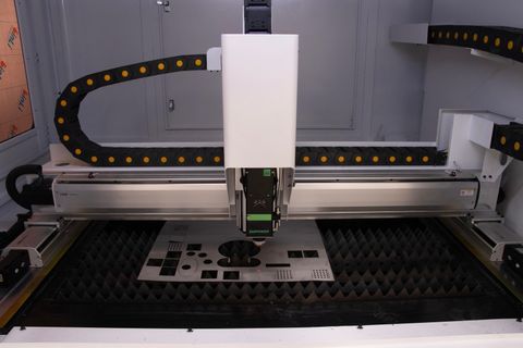
Wafer Fabrication Equipment Guide: Explore Types, Processes, and Industry Applications
Updated: November 21, 2026
Read More
Woffer Processing Equipment Guide: Explore Types, Applications, and Essential Industry Insights
Updated: November 19, 2026
Read More
Engagement Bands for Him Guide: Explore Style, Designs, and Essential Tips
Updated: November 18, 2026
Read More